Three days at SEMICON India 2026, and why we think the fabrication is the least investable part of the opportunity.
Most discussions of Indian semiconductors begin and end with the same question: can we build a fab, and by when. At 247VC, we have been deliberating this for a while now, and our team was at Yashobhoomi, Delhi to narrow down the question.
- What does the semiconductor industry actually buy, and at what point does a newer team from an Indian research institute become commercially relevant to a company like Applied Materials or Tata Electronics?
In the following position paper, we’ve consolidated our learnings from 3 days across 600+ exhibitors from 52+ countries. The short version is that the fab is one layer of a very deep stack, and it is the layer with the longest gestation and the highest capital intensity.
The layers around it are where we think the next decade of Indian value gets created, and most of them are still open.
Moore’s Law Is No Longer the Only Constraint
The economics of scaling changed well before the headlines caught up. Cost per transistor stopped falling around 28 nanometres, and every node since has bought performance at the price of margin.
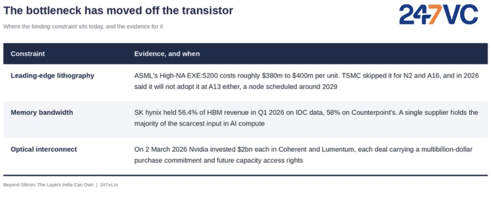
Read the first row again. The most profitable foundry in the world has now declined the most advanced lithography tool ever built across three consecutive nodes, on cost. When the leader stops buying at the frontier, the frontier has stopped being where margin is made.
Read the third row as the same signal from the other direction. NVIDIA's $4 billion combined investment in Coherent and Lumentum, alongside multibillion-dollar purchase commitments and future capacity rights, is a useful signal of where AI infrastructure bottlenecks are emerging. Capital does not move like that toward abundant inputs. Packaging capacity, substrates, thermal management and chemistry pure enough to be measured in parts per trillion are all being priced the same way.
India may not build an EUV scanner, and we should be realistic about that. But lithography is much broader than the scanner market suggests. Maskless and electron-beam technologies are slower and more capital-intensive, but they can be useful for prototyping, small-batch production, photomask-free manufacturing and compound semiconductors. Indian teams are already working on these technologies.
The bigger opportunity may lie beyond the scanner itself.
What we watched happen: electronics, AI, then 3D stacking, hence Photonics.
As we walked from booth to booth, conversing with industry leaders, it became easier to break down the evolution of photonic chips.
For three decades, more compute meant more transistors on a die. When that stopped working, the industry went sideways into packaging: chiplets, then 2.5D interposers, then true 3D stacking with hybrid bonding, where dies are joined at sub ten micron pitch with no solder bump in between. AMD’s 3D V-Cache and TSMC’s SoIC are built on the same concept. If you cannot shrink the transistor profitably, shorten the distance the signal has to travel.
That worked, and it moved the bottleneck again. Once the compute is dense, the constraint becomes getting data in and out of the package, and copper begins to lose. Conventional electrical interconnect runs at well over 30 picojoules per bit. Co-packaged optics on substrate targets under 5, and optical I/O on the interposer below 2. In data centres where expansion is limited by grid capacity rather than by capital, that is not an efficiency gain. It decides whether the next cluster gets built at all.
So the companies that spent the last decade on AI silicon and 3D stacking have spent the last two years buying photons.
AMD - It closed ZT Systems for $4.9 billion in March 2025 to own rack scale system design, acquired silicon photonics startup Enosemi 2 months later to build co-packaged optics in house, and has since backed Ayar Labs alongside NVIDIA. Merchant CPU and GPU silicon, to AI systems, to owning the optical interconnect, inside eighteen months.
NVIDIA - built its Quantum-X and Spectrum-X photonics switches on TSMC’s COUPE optical engines stacked with SoIC-X, then put capital into Coherent and Lumentum to secure the supply behind them.
Broadcom - shipped Bailly in 2024 with silicon photonic engines wrapped around a Tomahawk 5 switch, and its Tomahawk 6 platform uses COUPE based engines.
TSMC has taken the position everyone routes through, qualifying COUPE for pluggables in 2025 and folding it into CoWoS as co-packaged optics in 2026, with roughly 40% lower power claimed at the same speed.
Marvell is bridging the same gap through linear pluggables and photonic fabric roadmaps.Two things follow for India.
Photonics is not an adjacent bet, it is the next step in a migration these companies have already committed capital and roadmaps to, which makes the demand contracted rather than speculative. And the hard parts of it, fibre attach, laser integration, optical test and the packaging steps around them, are component and process problems rather than frontier lithography problems. This is the rare part of the migration that arrives as a supply chain question, and supply chain questions are ones India has answered before.
India’s Edge: Engineering, Talent and Scale
Every major economy now has a semiconductor programme, and most are competing for the same small number of fabs. What India holds is harder to assemble deliberately: roughly a fifth of the world's chip design workforce, a chemicals and pharmaceutical industry that has run purification and regulated documentation at scale for three decades, a domestic electronics market large enough to serve as a genuine first customer, and trusted partner standing inside supply chains that are diversifying away from a single geography.
India is now among the top in the world by deep tech company count at just under 7,700, and a distant third by capital, with roughly $1.65 billion raised in 2025 against $147 billion in the United States and $81 billion in China. The pipeline has been built. The financing infrastructure around it has not, and a meaningful share of Indian technical work is consequently incorporated and funded abroad.
The most consequential part of Semicon 2.0 was not the ₹1,27,500 crore headline. They were the notified guidelines, where a silicon fab carries a minimum project cost of ₹20,000 crore while a compound semiconductor, photonics or sensor fab requires ₹500 crore with 35 percent capital support, and design startups can access up to ₹15 crore. That is a policy calibrated to companies an early stage fund, an incubator or a university spinout can realistically support.
When do corporations actually begin to buy?
This is the question founders and investors ask most often and the one the ecosystem answers least precisely. A corporation does not engage because a company has raised a seed round. It engages at one of ten identifiable gates, and a different function owns the relationship at each.
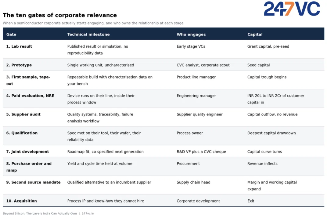
The trough runs from roughly month 18 to month 42. Four years to credible first revenue and four more to scale is the norm in this industry, and mistaking that curve for an execution failure is how sound companies are abandoned at month 30.
Three implications follow:
1) Corporate venture capital follows technical engagement rather than preceding it, so a conversation at gate two is exploratory while one at gate four is commercial. The trough is a financing problem rather than a scientific one, which makes the sequencing of DLI, C2S, ECMS and Semicon 2.0 support strategic.
2) India now has domestic buyers rather than prospective ones: CG Power short of leadframes and test sockets, Kaynes seeking advanced packaging know-how, Tata Electronics as the country's most significant first customer.
3) The fluorochemicals and industrial gas majors as natural acquirers of purification capability. Incubators and technology transfer offices should select projects against these requirements rather than publication potential.
Indian semiconductor exits to date have followed a consistent pattern: strategic acquisition between $40 million and $270 million, reached through a design win or a completed qualification. That is the base rate rather than the ceiling. A credible technical path to a listing exists wherever the product is consumed or licensed repeatedly rather than sold once, which is why the categories that reach public markets tend to be compound semiconductor power devices riding EV and renewables volume, consumables and specialty chemistry that earn revenue on every wafer, test hardware carrying installed base service income, and design IP earning royalties across multiple sockets. A business qualified into a single customer, however technically excellent, rarely compounds into that story.
Defensibility sits in the customer's qualification data
Defensibility doesn’t always come with technology and hard engineering. It is the customer's own qualification data, generated on their tool with their wafer over eighteen months and resident in their systems, which is why no procurement team removes a qualified supplier to save eight percent on unit cost. A qualified supplier of ordinary quality will outperform an unqualified supplier of exceptional quality for years.
This leads to a structural gap that, we thought, received little attention at the conference. India protects patents reasonably well and has no dedicated trade secrets statute, while semiconductor manufacturing runs on process know-how that is deliberately never patented, since a patent is a published recipe with a twenty year clock attached. Until this is legislated, Indian materials and process companies will continue to carry a valuation discount unrelated to the quality of their technology. For laboratories and university groups, it also changes what should be filed and what should be documented internally.
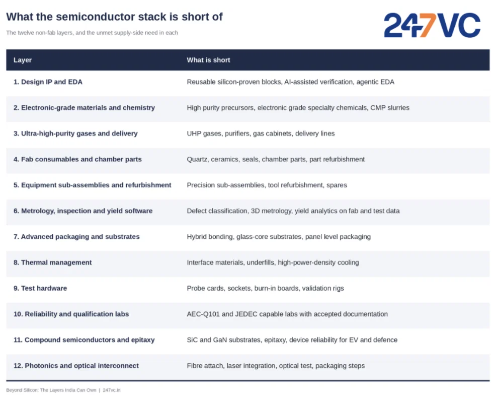
What the stack is actually short of
Everyone understands the semiconductor value chain, but pointing out relevant gaps from which industries can emerge from; requires an understanding of failures across EDA to verification, learning from scientists and working with corporations. These are the unmet needs 247VC has heard repeatedly on the floor, and our assessment of what India can realistically build at seed scale.
At 247VC, we screen across all12, and we underwrite where capital intensity, a domestic first customer and recurring revenue line up. Today that is test, photonics packaging, sub-assemblies and yield software.
Assembly and test capacity in India is expanding faster than the test supply chains that support it, which makes test hardware the most underserved opportunity in the country today. An unglamorous category, and an unavoidable one.
In conclusion: Stop Comparing Scale. Compare Access.
China is far ahead, and pretending otherwise is not Analysis. Big Fund III alone was registered at 344 billion yuan (about $47.5 billion), more than Funds I and II combined, and it is explicitly aimed at equipment and materials. China’s mature-node capacity will keep pressure on global legacy-chip prices for years. It also executes fast.
But India's advantage is not smaller scale. It is Access. India can license, partner and co-develop with ASML, Applied, Lam, TEL, Renesas and Infineon, while China is spending hundreds of billions to rebuild what export controls took away. Indian startups can sign JDAs in English, under an IP regime Western and Japanese corporates trust, inside a supply-chain club (Pax Silica) that China is structurally excluded from. India also starts without the burden of legacy overcapacity, and in advanced packaging, SiC, photonics and quantum enabling hardware, no one has a 30-year head start.
Our picture of India - 5 years from now and then 10 years from now.
In 2031: one operating 300mm fab at mature nodes running at meaningful but not full utilisation; 10-12 assembly/test units, of which three or four matter; the world's most credible second source for SiC epitaxy and power modules; and a real domestic gas and chemicals purification industry.
In 2036: a top-five destination for semiconductor equipment sub-assemblies and parts, a specialty photonics foundry, and at least one Indian-owned product company with over $500 million in revenue.
India does not need to replicate any other country’s model. It needs to become difficult to remove from the supply chain, which is both cheaper and more achievable.
A chip can be designed in Bengaluru, fabricated in Taiwan, packaged in Sanand, connected with photonics and sold into a data centre in Texas.
Our takeaways at 247VC, post Semicon India 2026:
Value has migrated permanently from the transistor to everything surrounding it, and India is arriving as that migration completes rather than after it.
Qualification rather than technology is the compounding asset, which means the companies worth building are designed from the first month to survive a forty month trough. T
he binding constraint on the Indian semiconductor industry is the structure of its capital rather than the quality of its science, which is a problem this ecosystem can solve considerably faster than it can build a fab.
If you are building something disruptive in this fast growing industry, Pitch to us.